Buck only steps down. Its switch, inductor and capacitor hold a duty cycle below one, so the output always sits under the input.
Boost only steps up. Energy stored in the inductor adds to the input voltage, and input current rises with the step-up ratio.
Buck-boost covers a battery that crosses the rail. The stage changes mode as the input passes through the target output.
Duty cycle explains the efficiency dip. Losses shift from switching to conduction as the input moves toward either extreme.
Worst-case input sets the heatsink. Size the thermal path at the lowest efficiency point, not at nominal voltage.
Protection is common to all three. OVP and continuous short-circuit recovery matter whichever topology is chosen.
Introduction
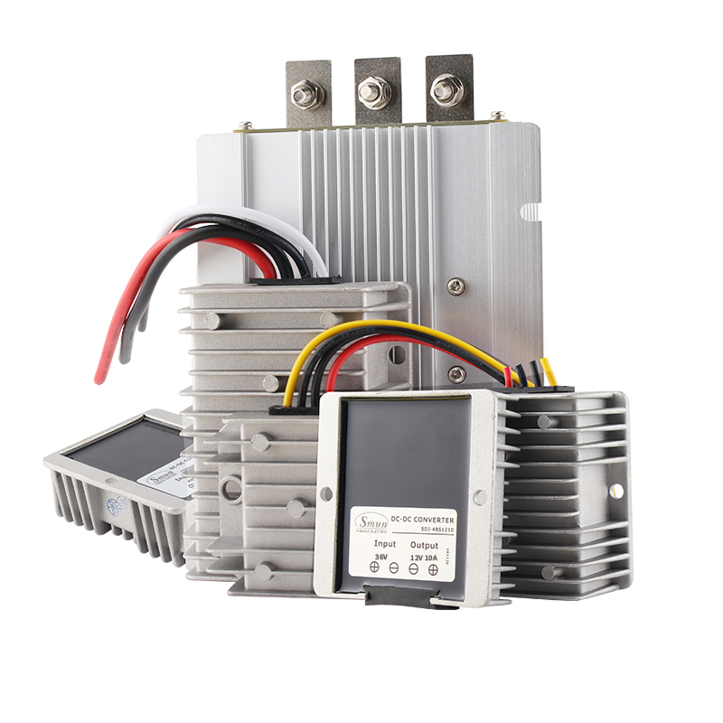
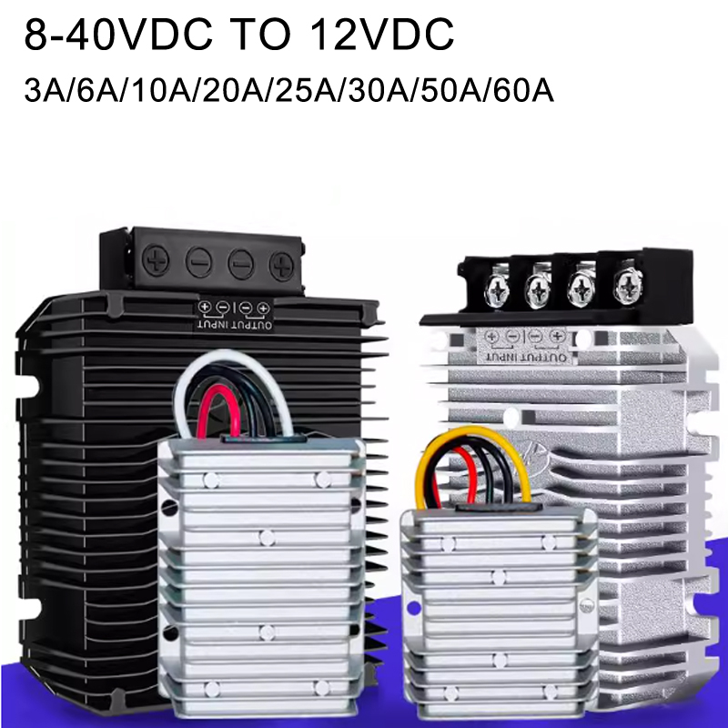
A buck converter is one of the most fundamental and widely utilized non-isolated DC-DC power supply topologies in electrical engineering. As industrial systems increasingly rely on complex DC power distributions—ranging from 48V battery banks to sensitive 5V microcontrollers—selecting the precise switching architecture is paramount. Whether you need to step voltage down, step it up, or seamlessly transition between both, understanding the technical distinctions between buck, boost, and buck-boost topologies ensures maximum efficiency, thermal stability, and prolonged component lifespan. A 8-40V to 13.8V boost-buck module is a working example of the third option in that list.
Buck vs Boost vs Buck-Boost: Topology Decision Matrix
When encountering a mismatch between your primary power source and your load requirements, choosing between a buck, a boost converter, or a combination architecture dictates the entire PCB layout and thermal strategy.
The Step-Down Efficiency of Buck Topology
The buck topology is engineered exclusively to step a higher input voltage down to a lower, regulated output voltage. It achieves this by rapidly switching a transistor (usually a MOSFET) to chop the input voltage, then filtering it through an inductor and capacitor network. Because the output inductor current is continuous, buck topologies offer exceptionally low output voltage ripple. This makes them the definitive choice for converting 24V industrial buses down to 12V or 5V to power logic circuits, sensors, and noise-sensitive communication modules, often achieving efficiencies exceeding 95%.
Stepping Up Power with Boost Topology
Conversely, the boost topology is utilized when the input voltage is lower than the required output voltage. It works by storing energy in an inductor while the switch is closed, and then releasing that energy in series with the input voltage when the switch opens, effectively "boosting" the voltage delivered to the load. Boost architectures are critical in applications like solar power tracking or stepping up a 12V automotive battery to 24V or 48V to drive heavy-duty industrial motors or specialized LED lighting arrays. Due to the discontinuous nature of the current delivery to the output capacitor, boost designs generally require more robust output filtering.
The Flexibility of Buck-Boost Architecture
A buck-boost design combines the capabilities of both previous topologies, allowing it to provide a strictly regulated output voltage regardless of whether the input voltage fluctuates above or falls below the target output. This topology is indispensable in battery-driven systems. For example, a 12V lithium-ion battery may read 14.4V fully charged but drop to 9V as it depletes. If the load requires exactly 12V, the buck-boost circuit dynamically shifts from stepping down the high voltage to stepping up the low voltage, guaranteeing uninterrupted operation until the battery is fully discharged.
Table 1: Buck, Boost and Buck-Boost Side by Side
Criterion
Buck
Boost
Buck-boost
Output against input
Always lower
Always higher
Above, below or equal
Duty cycle
Below one, set by the ratio
Approaches one at high step-up
Crosses the transition point
Inductor current
Continuous at the output
Discontinuous at the output
Continuous, with a mode change
Output ripple
Lowest of the three
Highest, needs larger capacitors
Moderate
Typical bus duty
48V or 24V to 12V
12V to 24V or 48V
12V battery held at 12V
How to Calculate Efficiency Across Wide Input Ranges (9-36V)
Integrating a buck boost converter requires a deep understanding of how varying input voltages drastically affect the system's thermal dissipation and overall efficiency.
Duty Cycle and Voltage Dynamics
Efficiency in switching regulators is intimately tied to the duty cycle—the percentage of time the main switching transistor remains "on" during each switching period. In a 9-36V wide-input system targeting a 12V output, the duty cycle shifts dramatically. When the input is at 36V, the converter operates in buck mode with a low duty cycle, which increases switching losses in the MOSFET. When the input drops to 9V, it operates in boost mode with a high duty cycle, heavily increasing conduction losses through the inductor and diodes.
Analyzing the Efficiency Curve
Engineers must not rely on a single peak efficiency number. Instead, the datasheet's efficiency curve must be scrutinized across the entire 9-36V spectrum. Typically, a buck-boost circuit exhibits peak efficiency when the input voltage is closest to the output voltage (e.g., inputting 12.5V for a 12V output), as this minimizes the work required by the switching elements. As the input voltage deviates toward the extremes (9V or 36V), efficiency will naturally dip.
Thermal Mitigation for Worst-Case Scenarios
Calculations must always account for the worst-case efficiency scenario. If a 100W converter operates at 92% efficiency at a 24V input but drops to 84% at a 9V input, the heat dissipation nearly doubles (from 8W to 16W of wasted heat). Thermal management strategies—such as selecting a larger extruded aluminum heatsink or ensuring adequate forced-air convection in the enclosure—must be designed to handle the 16W thermal load, preventing the converter from entering thermal shutdown during low-battery conditions.
Table 2: Where Losses Concentrate Across a 9-36V Input
Loss mechanism
Dominant when
Design lever
Switching loss
Input near 36V, low duty cycle, high frequency
Switching frequency and gate drive
Conduction loss
Input near 9V, high duty cycle, long on-time
Inductor DCR and switch resistance
Inductor core loss
Large ripple swing at either extreme
Core material and ripple ratio
Output capacitor loss
Boost mode, discontinuous output current
Capacitor ESR and bank size
Wasted heat at 100W input
92% at 24V gives about 8W; 84% at 9V gives about 16W
Heatsink and airflow chosen for the 16W case
Illustrative method only; not a product specification. Heat = input power × (1 − efficiency), following the 100W example in the text above.
Across a 9-36V input, an 8-40V to 12V boost-buck car converter keeps a 12V rail alive at both ends of the range, which is the case Table 2 is written for.
Design Examples: 24V to 12V and 12V to 19V Conversions
Applying dc dc buck and boost principles to real-world industrial scenarios highlights the practical application of these topologies.
24V to 12V Buck Conversion for PLCs
In factory automation, the primary control cabinet bus is universally 24VDC. However, many specialized sensors, human-machine interfaces (HMIs), and IT networking switches require a clean 12VDC supply. Deploying a dedicated synchronous buck converter provides the solution. By replacing the traditional diode with a second synchronized MOSFET, synchronous buck designs drastically reduce conduction losses, yielding minimal heat generation. This allows engineers to mount compact, unventilated 12V power modules directly onto DIN rails adjacent to the programmable logic controllers (PLCs) without risk of overheating the cabinet.
12V to 19V Boost for Mobile Computing
Consider fleet management vehicles equipped with ruggedized industrial laptops or specialized diagnostic equipment that require a 19VDC input. The vehicle's electrical system provides a fluctuating 12V (ranging from 11V to 14V depending on alternator state). A robust boost converter is utilized here. It steps the unstable 12V supply up to a tightly regulated 19V. In this design, ensuring adequate input capacitance is crucial, as the boost converter draws significantly higher current from the 12V side than it delivers to the 19V side, which can cause severe voltage droop on thin wiring harnesses if not properly buffered.
Implementing System-Level Protections
Regardless of whether a buck or boost topology is selected, robust protection circuits are mandatory. Over-voltage protection (OVP) prevents a failed switching transistor from passing the raw input voltage directly to the load. Similarly, continuous short-circuit protection (SCP) safeguards the converter from catastrophic failure if the output wiring is accidentally cut or shorted to ground, allowing the system to auto-recover once the fault is cleared.
Table 3: Two Worked Cases, 24V to 12V and 12V to 19V
Mastering the distinctions between topologies is a prerequisite for designing reliable industrial power architectures. While a buck converter offers unparalleled efficiency for stepping down voltages, and boost converters effectively elevate power, the buck-boost topology provides the ultimate resilience against wide voltage fluctuations.
By carefully aligning the specific topology with your load requirements and thermal constraints, system longevity is supported. Start by logging the input range at the connector, then read efficiency at both extremes of that range before the stage is fixed.
Q: What is the difference between a buck converter and a boost converter?
A: A buck stage produces an output below its input, while a boost stage produces an output above it. Both use a switch, an inductor and a capacitor; the difference is where the inductor sits in the energy path, which also decides whether output ripple is low or high.
Q: Can a buck converter raise the voltage?
A: No. A buck stage can only regulate downward, because the switch duty cycle is limited to less than one. Raising the voltage needs a boost or buck-boost stage, or a transformer-based design if a barrier is also required. No wiring arrangement on the output side reverses that limit.
Q: What input range forces a buck-boost design?
A: A source that can sit both above and below the output, such as a 12V battery reading 14.4V when charged and 9V when depleted, feeding a load that needs exactly 12V. A plain buck would drop out at the low end and a plain boost would lose regulation at the high end.
Q: Why does efficiency fall at 9V input?
A: Because the duty cycle rises toward one, so current flows through the inductor and switch for longer in every cycle and conduction losses grow. That is why the thermal design must be checked at the lowest input, not at the nominal bus voltage.
Q: Which protections should I check across all three topologies?
A: Over-voltage protection, continuous short-circuit protection with auto-recovery, and under-voltage lockout. The first stops a failed switch from passing the input to the load, and the third prevents erratic behaviour when the source collapses; check those rows against a wide-input part such as an 8-36V to 24V boost-buck module before approval.